A small-scale solution with a large-scale impact
Microchips are pervasive in today’s high-tech society, playing integral roles in the inner workings of your cell phone to your Keurig coffee machine.
A processing technology called CMOS, or complementary metal–oxide–semiconductor, made microchips economically feasible in the 1980s, said Sivasubramanian Somu, a research scientist in Northeastern’s Center for High-rate Nanomanufacturing.
A critical element in any microchip is something called an inverter — an electronic component that spits out zeros when you give it ones, and vice versa. “A transistor [the basic element in an inverter] is a simple, extremely fast switch,” Somu explained. “You can turn it on and off by electric signals.”

A computer chip using the molybdenum disulfide inverter. Photo by Brooks Canaday.
In the early days of computer technology, mechanical switches were used for computational operations. “You cannot achieve fast computations using mechanical switches,” Somu said. So CMOS, which used electric signals to turn the switches on and off, represented a significant advance in the field.
But despite its relative economy, a CMOS fabrication plant still costs about $50 billion, according to Somu. “We needed an alternative, cost-effective solution that still can compete with CMOS at the foundry level,” he said.
CHN’s proprietary “directed-assembly” approach is that alternative solution. Instead of requiring several fabrication steps of adding and removing material, as in the case of CMOS, directed assembly is an additive-only process that can be done at room temperature and pressure. A fabrication facility based on this technology, Somu said, could be built for as little as $25 million.
This cost savings would make nanotechnology accessible to millions of new innovators and entrepreneurs, unleashing a wave of creativity the same way the PC did for computing, said Ahmed Busnaina, the William Lincoln Smith Professor and Director of the NSF Center for High-rate Nanomanufacturing.

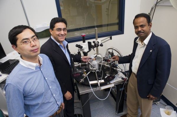
A custom probe station that varies temperature and atmospheric pressure to measure the electrical properties of materials at the Center for High-rate Nanomanufacturing. Photo by Brooks Canaday.
But creating a nanosized inverter is easier said than done, added Jun Huang, a postdoctoral research scientist in the center. Researchers have using materials like graphene and carbon nanotubes for creating inverters, but none of these has worked well on its own. Creating a nanosized inverter made up of different nanomaterials with excellent properties, Huang said, can result in excellent complimentary transistors.
Using the directed-assembly process, the team created an effective complimentary inverter using Molybdenum disulfide and carbon nanotubes. “At the nanolevel,” said Huang, “molybdenum disulfide occurs in thin, nanometer-thick sheets.” At this scale, he noted, the material begins to demonstrate transistor characteristics critical to the construction of a good inverter.
The success represents a step toward CHN’s ultimate goal of enabling small- and medium-sized businesses to develop new, microchip-based technologies. The results of their research were reported in a recent article in the journal Nanotechnology.
View selected publications of CHN researchers in IRis, Northeastern’s digital archive.