Bicoastal Institute for NanoSystems Innovation launches at Northeastern University
NanoSI is located on the Boston and Oakland campuses. It aims to reshape “the landscape of chip-level technology advancements and applications.”
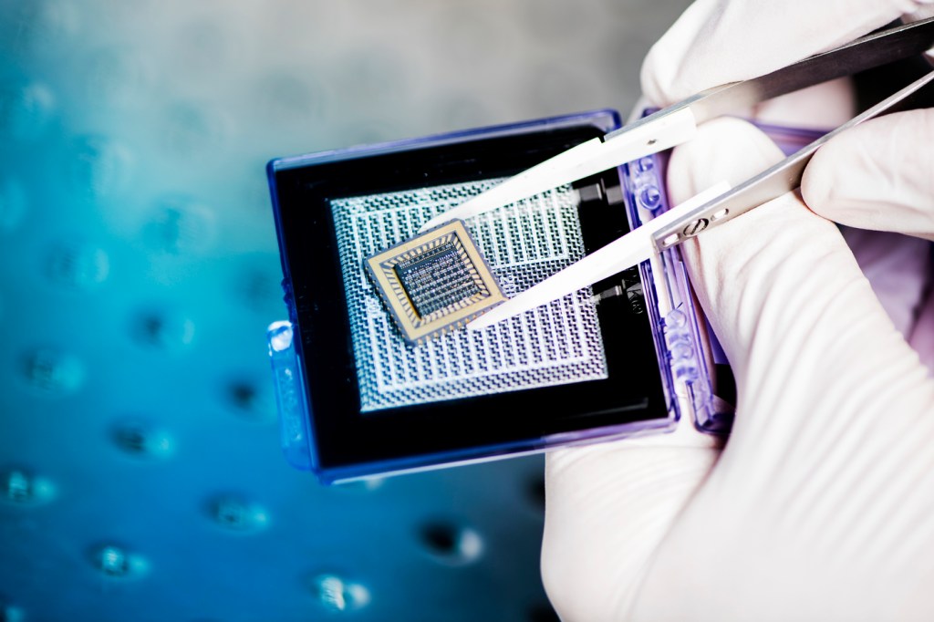
A medical device that can help determine if you have cancer, but can fit on the pad of a fingertip. Miniaturized radio frequency devices to enable 5G technology and beyond. Wearable sensors and implantable technology. Quantum computing.
These are just some of the futures made possible by nanotechnology — technology measured on the scale of a nanometer, one-billionth of a meter.
Now, Northeastern University is launching the first-of-its-kind Institute for NanoSystems Innovation (NanoSI), straddling both coasts of the United States.
NanoSI is co-directed by David Horsley and Matteo Rinaldi, both professors of electrical and computer engineering (and who, earlier this month, received the 2024 Global Network Accelerator Award).


‘A serious investment’
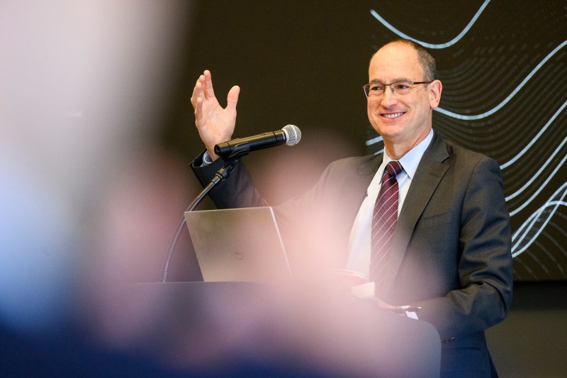
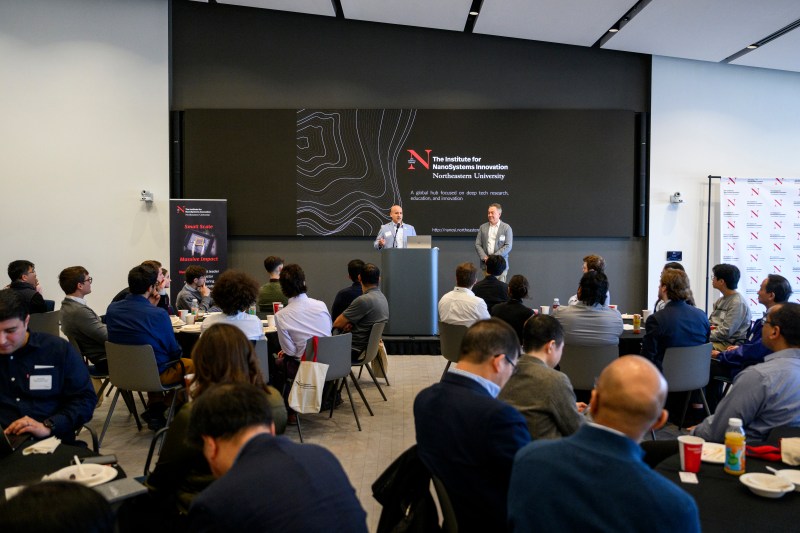
At a launch event on the Boston campus Friday morning, David Luzzi, senior vice provost for research and vice president of the Innovation Campus in Burlington, Massachusetts, described NanoSI as “a serious investment of the university, and it’s really built around things that are truly inspiring.”
“The first is great leadership talent,” he continued, gesturing to Horsley and Rinaldi. “The second thing is that these leaders had a vision that dates back” to the Northeastern University SMART Center, which Rinaldi directs. Rinaldi “built the plane while it was flying,” Luzzi said.
Nano-scale systems are by nature very, very small. To put “one-billionth of a meter” in perspective, a strand of human hair is between 80,000 and 10,000 nanometers wide, while a strand of human DNA is only 2.5 nanometers wide, according to the National Nanotechnology Initiative.
NanoSI will develop technologies on this scale, driving innovation and miniaturization across a wide range of functions. They aim to reshape “the landscape of chip-level technology advancements and applications,” the organization writes.
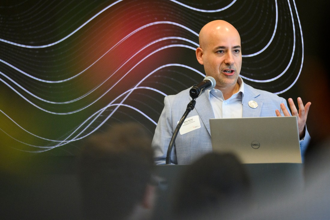
Rinaldi, director of the new institute, noted how this is likely “the first academic institute in the country focusing on semiconductors that is bi-coastal,” thanks to “the global university system that has been built here at Northeastern.”
“Semiconductors,” he also noted, are the “brains and senses of modern electronics.”
Horsley, deputy director of the institute, was visiting Boston from Northeastern’s campus in Oakland, California. He described his excitement for a “new facility that’s coming online in Oakland,” as well as new faculty hiring with specialties in microsystems engineering.
Horsley also pointed to the fact that NanoSI is now the largest center for micro-electromechanical systems (MEMS) research in the United States.
NanoSI will feature a spread of experience, from established researchers with decades of experience to young faculty getting established in — and disrupting — their field. “When you engage with us,” Horsley said, gesturing to himself and Rinaldi, “you also get those people who are early in their career and devoted 100% to their research.”
NanoSI already boasts 22 faculty and over 150 other researchers.
Featured Posts
Confronting new challenges
Rinaldi says there is a bottleneck in the semiconductor industry that emerges from a shortage of talent on one side and, on the other, misalignments between research and development laboratories, “where the innovation typically initiates,” and large-scale manufacturing and fabrication.
“These new technologies come with new challenges,” he explains. “Our objective is to really open this bottleneck” by leveraging Northeastern’s experiential learning and co-op programs to provide “hands-on training of the workforce,” its global network of campuses and researchers and by “providing industry-compatible” instruction to “bridge that lab-to-fab gap.”
Dana Weinstein, professor of electrical and computer engineering at Purdue University, gave a keynote on the state of the semiconductor industry and the challenges it currently faces.
Weinstein is currently serving as a special advisor on research and development for the CHIPS and Science Act — Creating Helpful Incentives to Produce Semiconductors — in the executive office of the president.
Calling in from the Eisenhower Executive Office Building in the White House, Weinstein noted how “onshoring our advanced semiconductor manufacturing [and] investing more aggressively in the future of semiconductors” were both key policy points for the Biden administration.
“It’s wonderful to see institutes like NanoSI that are taking the lead and looking to bridge all of those critical gaps in knowledge, in technology and in infrastructure,” she said, “including these public-private partnerships.”
“The idea is to create these hubs across the country” involved in semiconductor research and innovation, Weinstein said. “Boston and the Bay Area play a critical role in that.”

Miniature medicine
After Weinstein’s keynote, Soner Sonmezoglu, assistant professor of electrical and computer engineering, gave a presentation on some of his current research under the NanoSI umbrella.
The first was a minimally invasive catheter that facilitates MRI-assisted prostate cancer diagnoses, using a device less than two millimeters wide.
Sonmezoglu also described how he and his team are developing “implantable, wireless microsystems” that don’t have to be implanted “through major surgeries,” he says. “We can implant these devices into the body through a needle.”
NanoSI already has a presence on three Northeastern campuses with a 15,000-square-foot laboratory in Boston and a new 20,000-square-foot clean room in Burlington.
Thanks to Northeastern’s Oakland campus, “We can now say, ‘Well, this bi-coastal thing is done,’” Luzzi said. “Now let’s take it global.”


